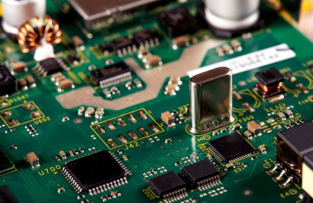
Not every electronic device is built the same, and that is why one size circuit board for all often does not cut it. If you ask questions how to adjust the PCB to suit your project, you are definitely not alone. Whether you improve the prototype, increase production, or only aim for better reliability, understanding the available options can be very helpful.
Adjusted PCB design tends to open a lot of flexibility – size, layer, complete, and more, all of which can affect how well your board performance is under pressure. So, in this guide, we break the key decision behind the customization of the PCB board, showing what is really important without all unnecessary feathers. If you want to know about the next practical steps, we PCB assembly The page might be a good place to start.
Size and shape
Getting the right dimension is not just about squeezing the board into the case. This is more about ensuring that it works well in its environment, whether it is a handheld device or part of a larger system. PCB board customization often starts here – leaks length, width, or outline to match whatever housing or functions you have.
The standard square or standard rectangle tends to be easier and cheaper to produce. Which says, special profiles can sometimes be a better call, especially if you design it for items that can be worn, a strange -shaped cover, or an integrated sensor module. The goal, usually, is to achieve a balance between available space and reliable performance. So, if your design feels a bit pinched, this might be your first stop for adjustment.
Number of layers
After the shape is sorted, the next thing to think about is how many layers actually need PCB. This is not only a number game – this directly affects the complexity, signal quality, and production costs. A single layer board may be good for a simpler device, but if your circuit does more than just the basis, you might see multi-proof settings.
The trick is to find out what your layout demands. The four -layer board, for example, often gives you better control over the signal path, which can help with noise and disturbance. This is part of what makes the PCB layer calculate the main custom choices. If your design feels narrow or your signal collides, adding one or two other layers may sort it.
Material choice
The material made by your board is no more than just holding components in places – quite a lot forms how it handles heat, stress, and electricity. Most PCB designs are adjusted using FR-4 as a basis. This is difficult, stable, and affordable. But that is not the only choice.
Polyimide tends to appear a lot when the flexibility or higher temperature resistance is needed, especially in space or automotive teeth. Then you have a PTFE and other special laminates that offer better performance at high frequencies. So, choosing between the types of PCB material is not just a technical preference – this is about what the council needs to survive and function properly. Is your circuit in the laboratory, car, or that can be worn, the right basis makes all differences.
PCB thickness
Your PCB thickness is not just about how much it feels in your hands – it affects everything from mechanical strength to current flow and heat handling. Too thin, and maybe too flexible. Too thick, and you can experience housing problems or installation.
In most PCB designs that are adjusted, the right thickness depends on the needs of the current carrier, the heat dissipation, and the connector you are using. The type of detail that is silent can make or destroy performance. If you are not sure where to start, our guide PCB thickness Crush without jargon – very worth seeing if you weigh your choice.
Component placement
Where things happen on your PCB as important as what you are wearing. Intelligent layout is not about squeezing everything to angle – this is about ensuring heat can come out, the signal remains clean, and components are easily accessible or replaced later.
Poor placement tends to cause headaches, excessive heat, signal disorders, even the delay of assembly. That is why customization of PCB boards usually involves a little thought about distance, orientation, and stomach. For example, maintaining a separate path and signal can help cut noise. Grouping the related section can simplify testing. This is one area where a little view ahead as long as the design tends to save a lot of pain on the phone.
Final surface
After the board is shaped and placed, the surface is complete is what makes it ready for solder-and helps him survive. This thin outer layer protects copper and affects how easy the component is attached during the assembly. So, choosing the right one is really more important than what is seen.
HASL (Hot Air Soldering Leveling) is often the goal of running with a budget, but not always ideal for the smooth pitch components. Enig (Electric Nickel Soaking Gold) gives a more flat end result, more durable – better for the right build. OSP (Organic Sutderability Preservative) is in a place in between. Your choice usually depends on the cost, life expectancy of shelves, and production volume. For those who are looking for the PCB surface finish option, this is a quite practical decision with real consequences.
Through the type
VIAS is a small hole that allows signals to run between layers, and in adjusted PCB designs, the type you choose can shape the performance and production costs. Vias through a hole is the most common and easiest to recognize. They passed the board, from top to bottom.
Blind Vias connects the outer layer to the inner without punching the entire board, while Vias is buried completely inside, hidden from both surfaces. For a simpler design, holes through holes are usually successful. But when the space becomes fast or you laying, knowing your PCB through the type can help tidy up everything.
Impedance control
If your circuit handles the signal quickly thinking about high-speed data or radio-control frequency impedance starts to be important, many. Without it, signals can be distorted or reflected, which leads to better performance problems you avoid.
The PCB board customization section focuses on matching the width of the track, distance, and material with the frequency and speed of the signal. This is not something that is needed by every project, but for anything that involves high -speed RF or digital lines, usually cannot be negotiated. Doing it correctly tends to mean a cleaner communication and fewer unexpected problems on the phone.
If the PCB board customization feels extraordinary, don’t hesitate to reach. We are here to help with the size, layers, materials, and more. contact us Today at Altimex for expert guidelines and ensuring the success of your project with PCB solutions that are designed perfectly.
Posting how to adjust the PCB board first appeared on Altimex.
Game Center
Game News
Review Film
Berita Olahraga
Lowongan Kerja
Berita Terkini
Berita Terbaru
Berita Teknologi
Seputar Teknologi
Berita Politik
Resep Masakan
Pendidikan
Berita Terkini
Berita Terkini
Berita Terkini
review anime
Gaming Center
Originally posted 2025-05-21 19:08:20.